Wish you all great discoveries and a lot of fun with science.
Sergey Frolov, Academic Community Member
Wish you all great discoveries and a lot of fun with science.

Several young theorists from Delft and Maryland have put together an online course on ‘Topology in Condensed Matter’.
https://www.edx.org/course/delftx/delftx-topocmx-topology-condensed-matter-6331#.VIhbGzHF-So
The course starts February 9, reserve your spot now! There is no room for everyone on the internet.
Finally the ultimate geeks of the internet caught up with topological quantum computing. (You would think they would be the first to figure it out)
PhD Comics interviews Caltech theorists Gil Refael and Jason Alicea on the subject of anyons. Our Delft device makes a cameo.
And here is a recent article from MIT Technology Review talking about the hardware aspects of this:
http://www.technologyreview.com/featuredstory/531606/microsofts-quantum-mechanics/

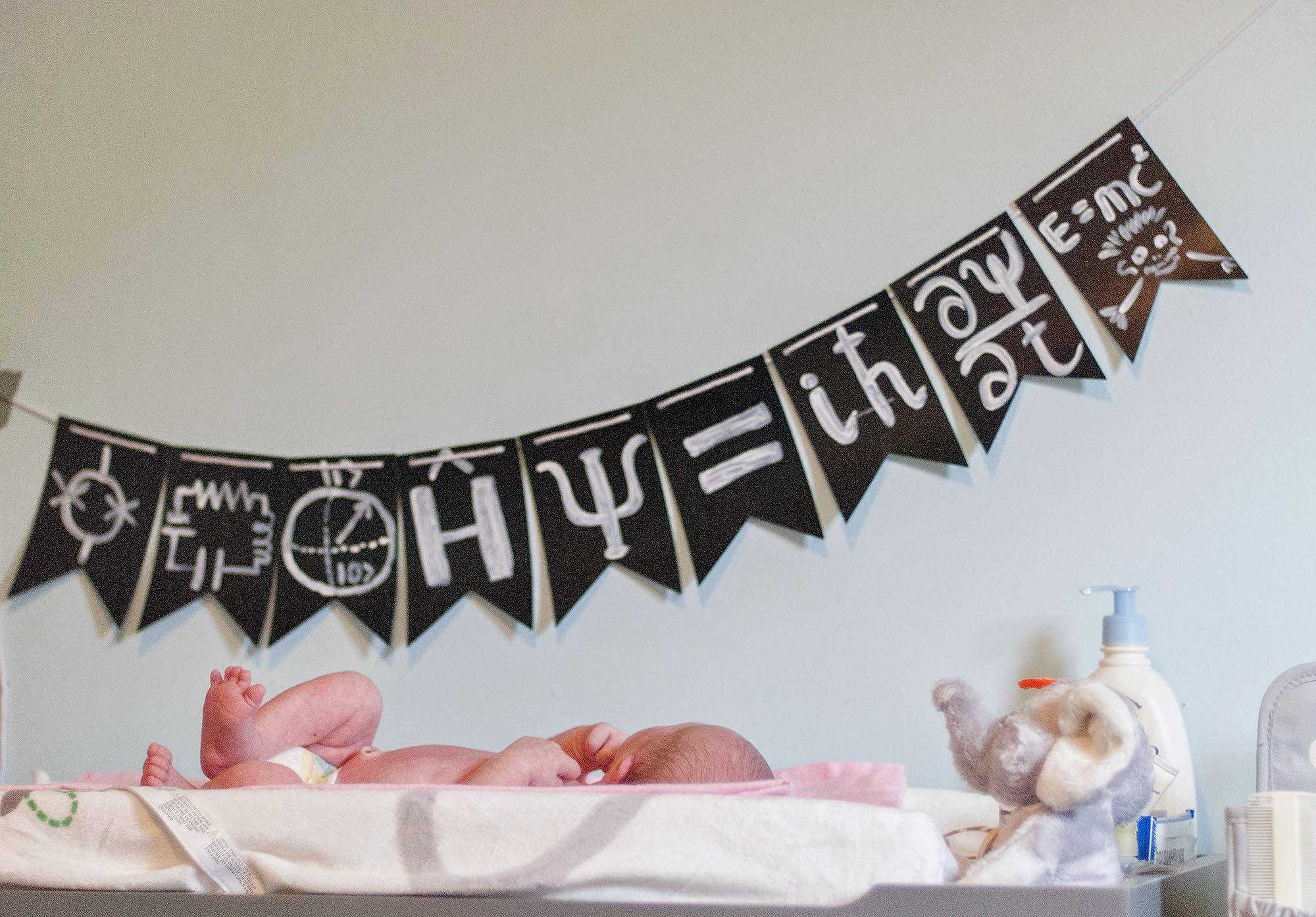
Long-long time ago when I was a graduate student chasing, as most of us, a wild vision of my great advisor, I found myself trying again and again to fabricate devices in the cleanroom, cool them down, measure them – with no luck! My aspiration was to observe amazing never before seen physics, yet I could not even see the things from many decades ago like the supercurrent. At that point, as an act of Universal discourse, I printed a small request on a sheet of paper and posted it on the wall in front of my measurement computer. It said ‘DEAR SOMETHING, PLEASE WORK!’. Time passed, and through sweat and pain the god of Something bestowed her benevolence on me. I saw the supercurrent – I was so happy I called my advisor late in the evening. (I haven’t been so excited since I have spotted a guy named ‘Larry Cooper’ at my first March Meeting and took him for Leon Cooper, the discoverer of Cooper pairs and of mini-Cooper cars).
Anyhow, when I visited my old lab in Urbana last year my prayer was still attached to the wall. Only it was the second one. To the God of Everything.
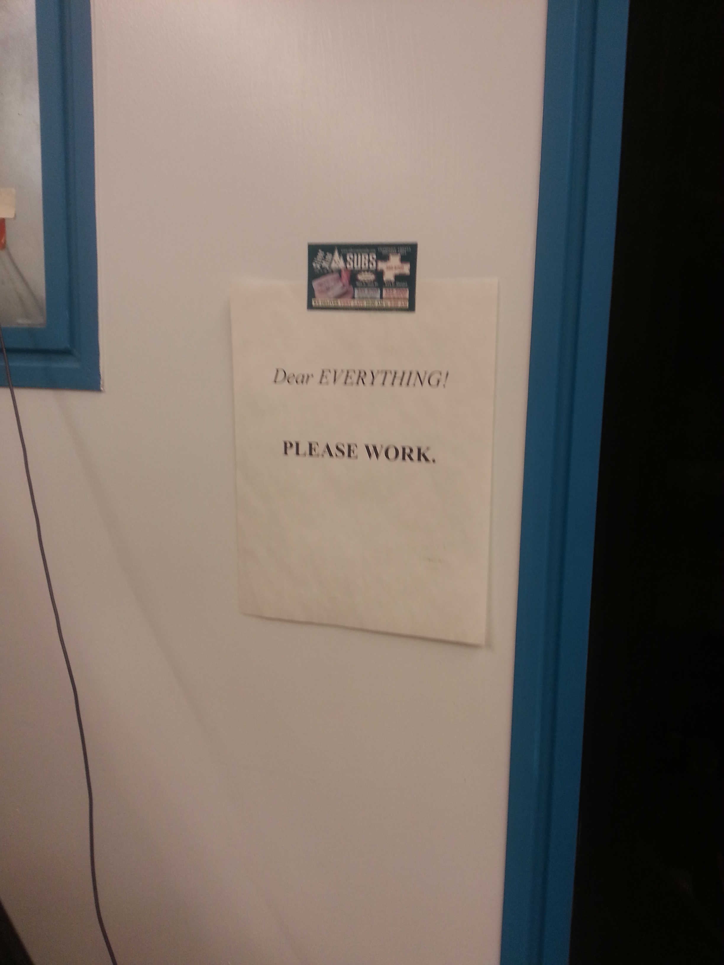
For an experiment to be successful, EVERYTHING has to work. And for me supercurrent was only the beginning. Once you got something working, your appetite and your paranoia grow exponentially. We are at this point right now at Pitt. As soon as everything works, something will come out.
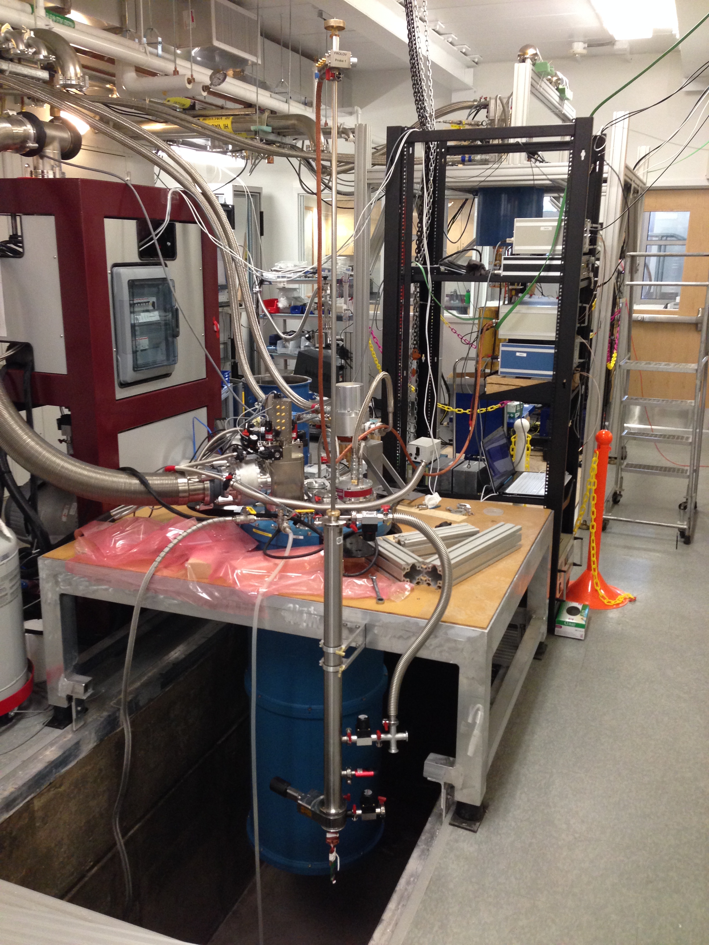
The construction of a facility to liquefy helium has started in the back of the Physics building at Pitt. Liquid helium is the blood of most cryogenic experiments, it becomes liquid at 4.2 degrees Kelvin (which is cold) and simply immersing your experiment into this liquid gives you this low temperature.
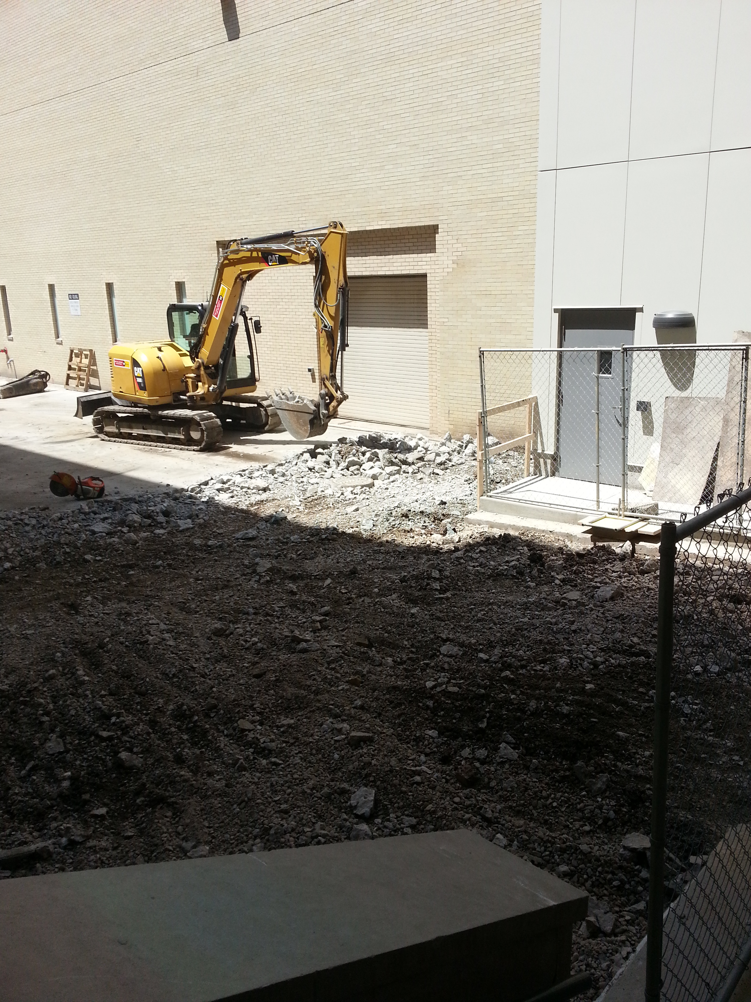
So far the project literally only scratched the surface, in a short while a new space will be added to host this helium equipment. Pitt is very much forward-looking with this new construction. The prices of helium gas have been going up, and combined with liquefaction costs they more and more often make low temperature experiments simply unaffordable. What makes our liquefier cost-effective is that it comes with a recovery system: helium that boils off in the labs around campus will be pumped back to the liquefier rather than lost into atmosphere. Our lab was already constructed with recovery plumbing, so we will be able to use local organic liquid helium from a friendly liquefactor down the street.
The last few months our group has dedicated to nanofabrication. It is a lot like cooking in that we talk a lot about recipes, and we get to wear white overall suits which make you feel like a chef. It is however much more strict than cooking as every recipe has to be perfectly tweaked for the final result to work. I have decided to explain how nanowire devices come about cookbook-style.
Ingredients: 1 chip nanowires, 1 2” wafer silicon substrates, PMMA and MIBK, titanium, gold, hafnium oxide, acetone and isopropanol to taste.
The main ingredient is a nanowire. It is of course highly recommended to get the best and fresh nanowires, here we shall use indium antimonide wires grown in Eindhoven, but we also have other great recipes for example with silicon-germanium grown in Los Alamos. Great, so put nanowires aside, we will need them a bit later.
We start by preparing the substrates. Here again our recipe is a little extravagant as we shall be using substrates from France, but you can use substrates from your local market. We prepare a whole 2” wafer and then cut it into smaller pieces for final devices. The fist step is to fabricate markers, they are needed as coordinates and reference points for other layers of nanofabrication. They are produced by electron beam lithography which can define the cross-shaped patterns shown below. Make sure you spin PMMA before doing lithography, and then develop it in MIBK for about a minute.
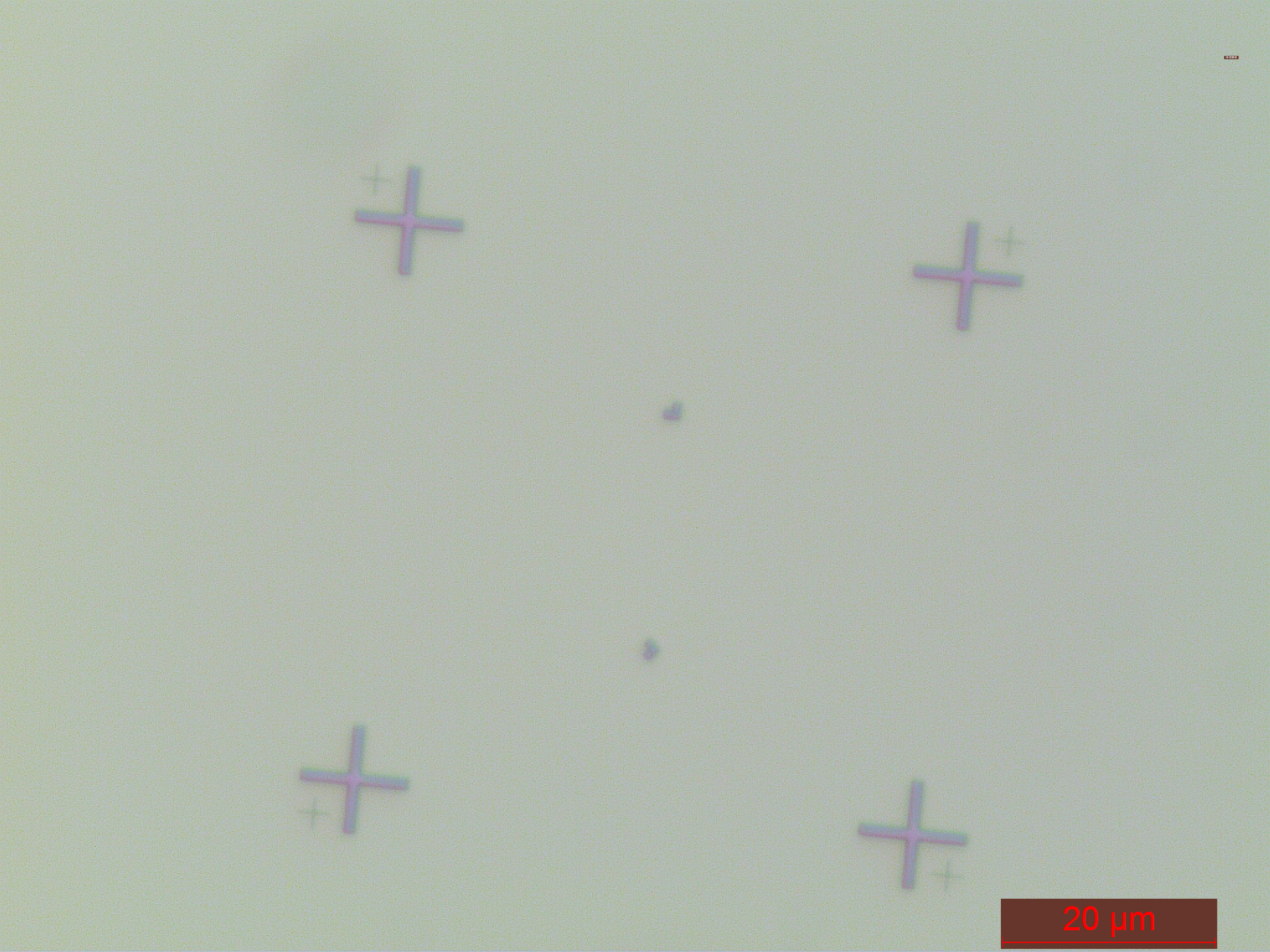
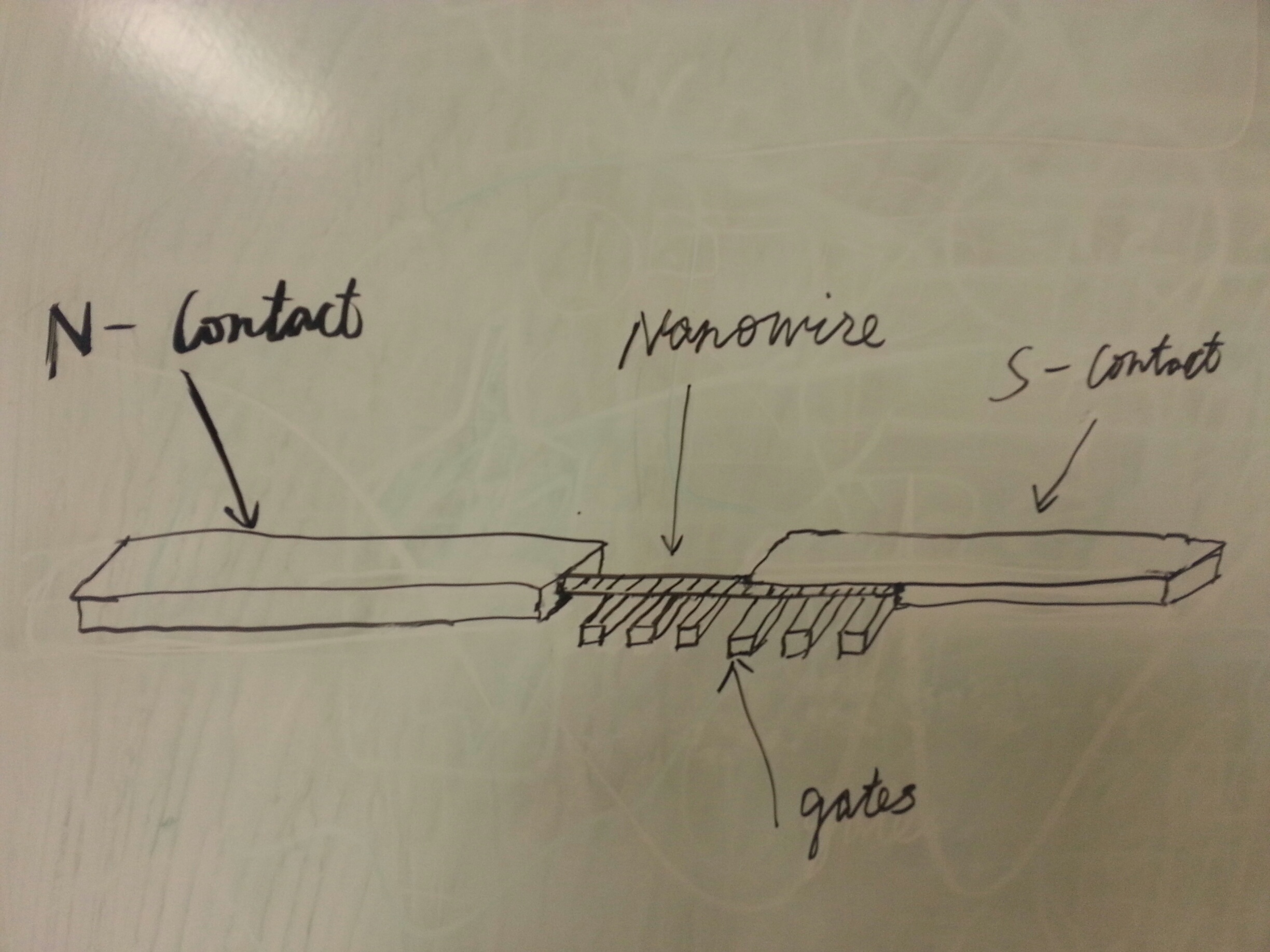
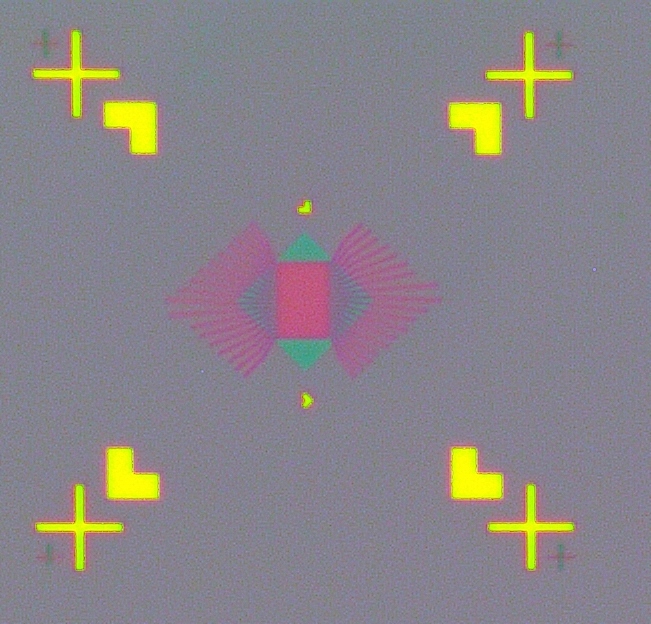
The final pattern is obtained by evaporating titanium and gold and liftoff of the rest of PMMA. You need to evaporate these metals in vacuum, so make sure you have an electron beam or a thermal evaporator. While these crosses are relatively large, the meaning of nanofabrication really comes to life when we form the layer of gates, also by electron beam lithography. These are parallel lines that can be as thin as 20 nanometers. In the picture below you can see an image of gates in a standard microscope in pink. The pink rectangle in the middle is so dense that individual gates cannot be resolved. You also see yellow gold markers in the corners, they were used to position the gates in the center. A cyan rhombus is a layer of hafnium oxide dielectric which will eventually separates gates from nanowires to help avoid shorts. This layer is produced by atomic layer deposition, in which organic molecules carrying hafnium atoms coat the subtrate and then disintegrate leaving behind a single layer of oxide.
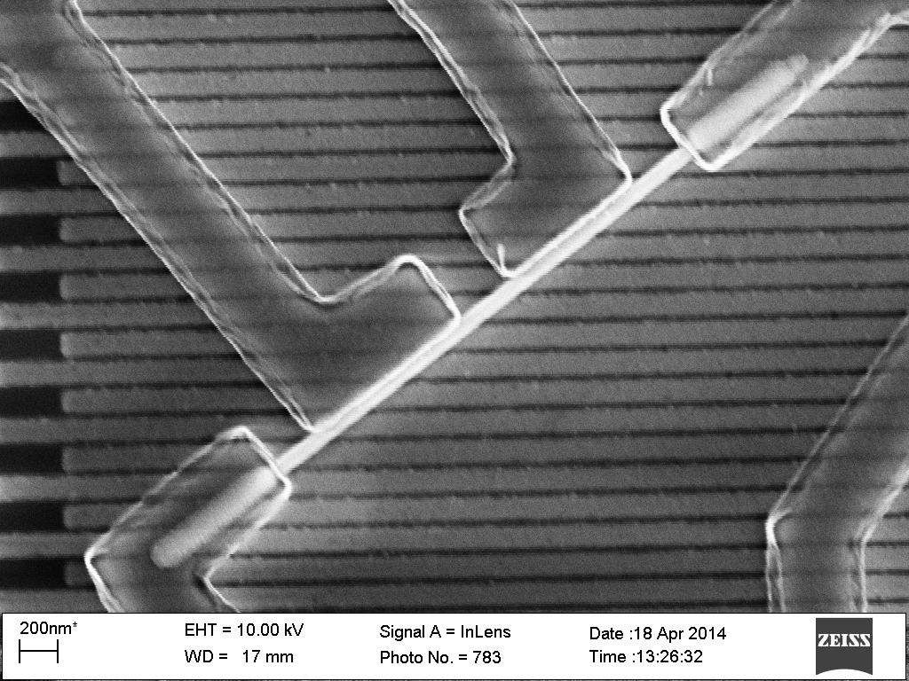
After these steps our substrates are cut into 10 mm squares and get shipped from Grenoble to Pittsburgh. Here we take the Dutch nanowires and place them one by one onto the gates, as shown in this video.

The nanowire is a bright white object in the center. You can also see better the gates in the picture above because this picture is taken with a scanning electron microscope. Although these pictures are always in grayscale reflecting the color of electrons.
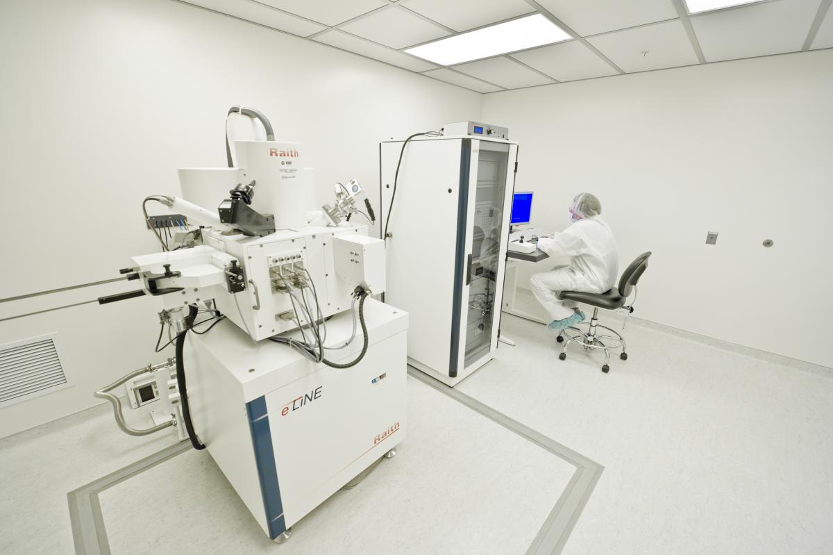
All this is done in the cleanroom which looks like this:
The last step is to contact the nanowire with electrodes. We take a picture of exactly how the nanowire lies on the gates, and then design contacts (in a computer) to cover the tips of the wire and its sides. We will later pass current and measure voltage across the nanowires through these contacts, that is the experiment part of our work.
We use the electron beam lithography machine shown in the picture above to write the pattern of contacts on top of the nanowire. The substrate and the wire are coated with PMMA which is a polymer that gets broken down by a beam of electrons during lithography. Where the molecules of PMMA were broken they come off in MIBK leaving openings. Metals like titanium and gold can be deposited in those openings.
Finally, rinse the chip in acetone and isopropanol and you are ready to measure! Enjoy your experiments.
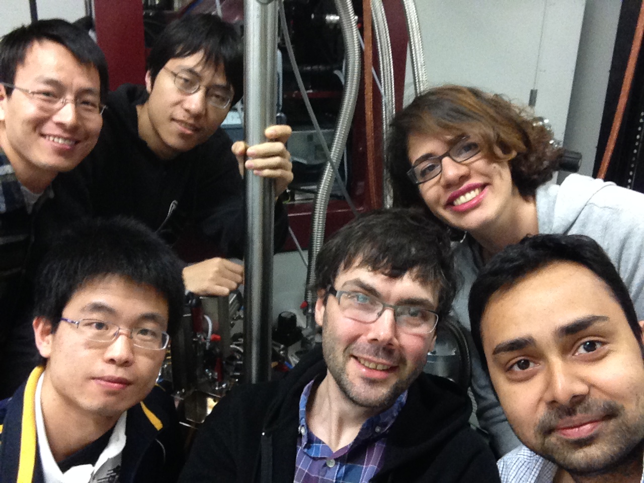
snapped during a group meeting this morning. Left to right: Jun Chen, Zhaoen Su, Peng Yu, SF, Azarin Zarassi, Dharam Patil.
The first discovery out of Frolov lab.
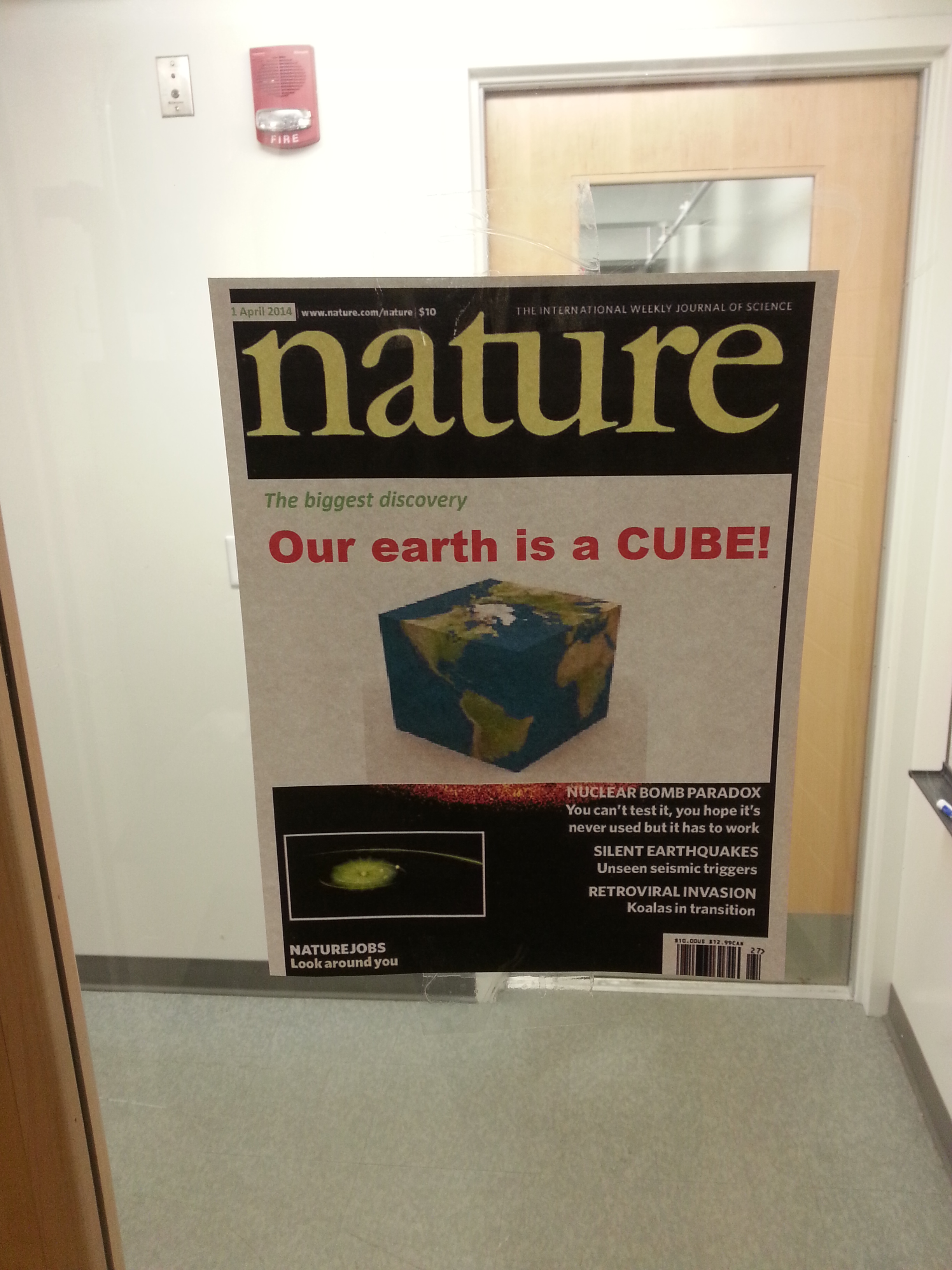
We tried to submit it to Physical Review B, but the referees said that a cube is topologically equivalent to a sphere, so there is nothing new.
Last year we have started PQI, originally known as ‘Pitt Quantum Initiative’. This year, with support from the University this initiative has began transforming into ‘Pittsburgh Quantum Institute’ that will embrace quantum research at Pitt and Carnegie Mellon. In line with the tradition started last year, we are going to have a conference that will bring together some of the leading researchers in the field of Quantum Technologies.
From http://pqi.pitt.edu/ :
Pitt Quantum Initiative event on “Quantum Technologies”, 9-11 April 2014
Our second annual PQI event will be held from Wednesday April 9th to Friday April 11th this year. The first two days will be held in the University Club, and a final morning session will take place in the Cathedral of Learning.
As with last year’s event, we will again cover a broad range of areas, including
Quantum Chemistry
Quantum Materials
Quantum Phases and Phase transitions
Quantum Transport
Quantum Gases
Quantum Devices
The program will present a broad range of research being performed in these fields, and will feature prominent invited keynote lecturers, as well as highlighting current research in the PQI. All of the talks will be colloquium-style, and accessible to a broad range of people in quantum-related fields.
Invited Lecturers
Roi Baer (Weizmann)
Garnet Chan (Princeton)
Michel Devoret (Yale)
David DiVincenzo (Aachen)
Greg Engel (Chicago)
Leticia Gonzalez (Vienna)
Jack Harris (Yale)
Evelyn Hu (Harvard)
Randy Hulet (Rice)
Alfred Leitenstorfer (Konstanz)
Ana Maria Rey (JILA)
Seigo Tarucha (Tokyo)
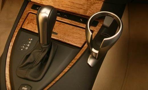
Fridge is not a luxury, but a means of refrigeration. Yet it costs like a luxury car, in the ballpark of those fancy italian Maserati’s and Lamborghini’s. In our case the fridge was even built by a company with italian roots. However, what would you say if your Maserati came without a cup holder? Even a basic one like this…
Well, our fridges came without probe holders. Probes are very useful for quick sample turnaround. They are long sticks which can be used to load samples into a cold fridge thereby shaving off days from the sample exchange cycle. The probes are long and awkward to handle. So we talked to our machine shop in Physics at Pitt to add a probe holder to the system. And they came up with a nifty design:
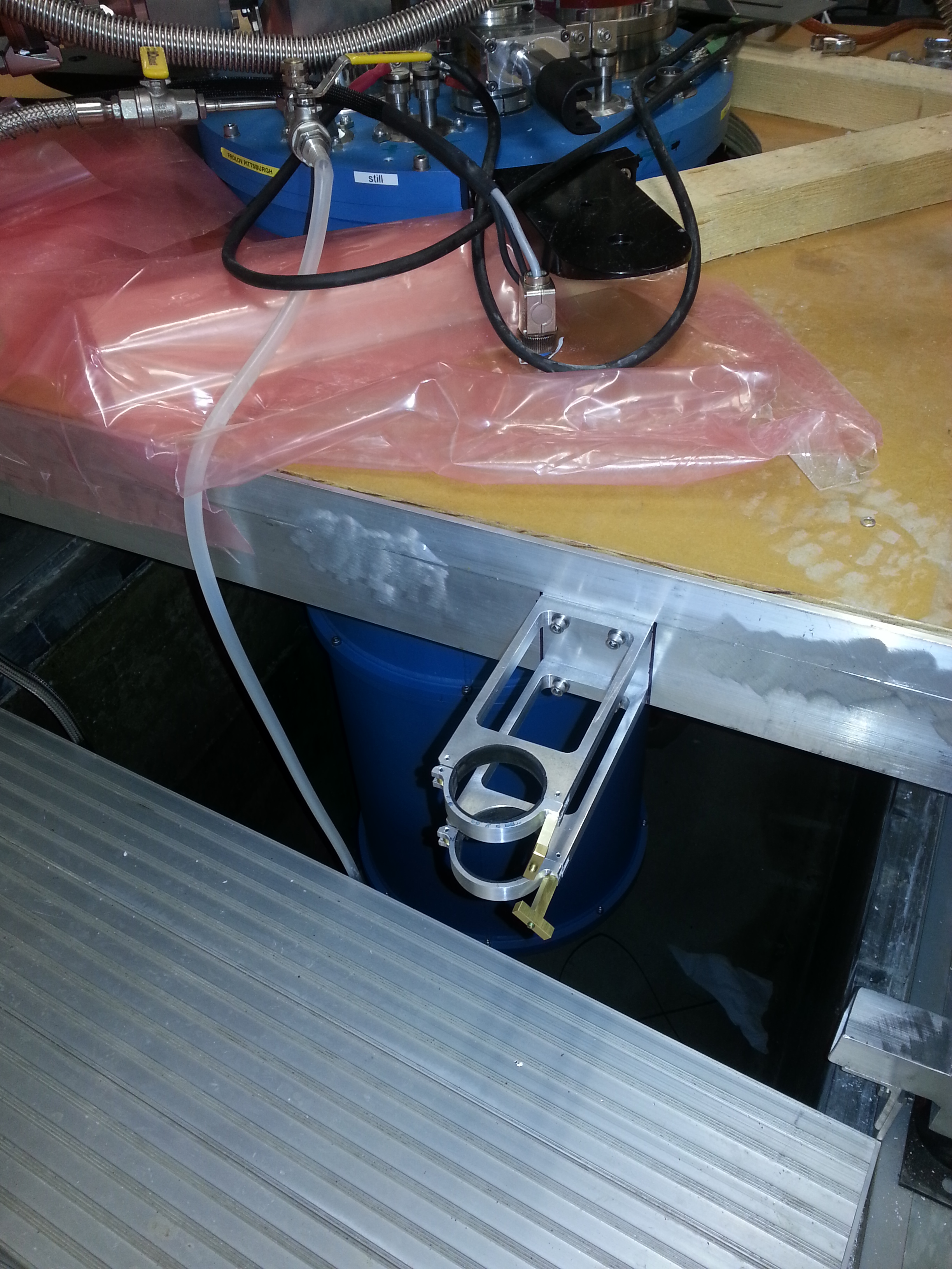
And here is how it looks with the probe being held by it:
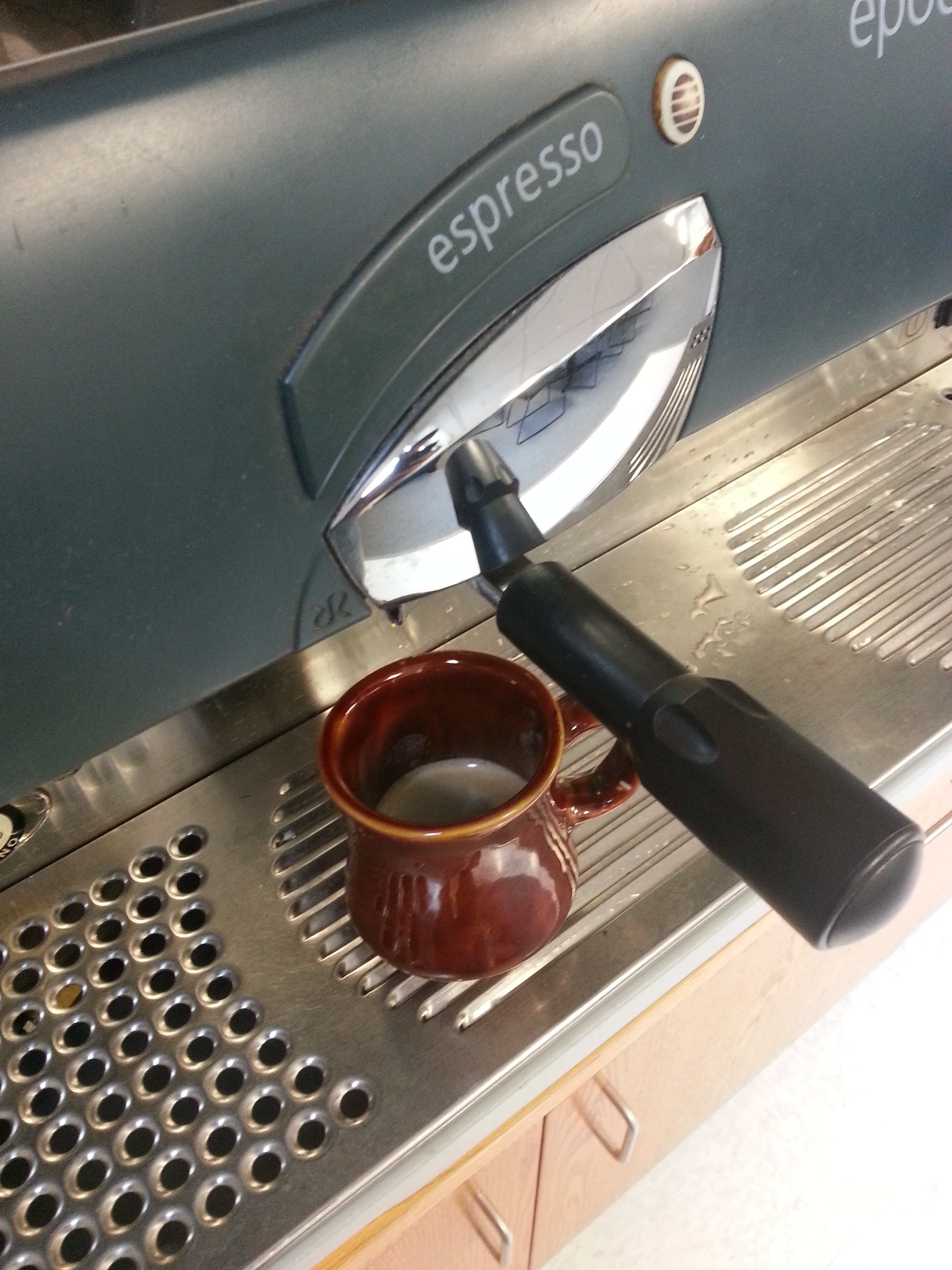
Here is a picture of the first cup of espresso. We are now tuning the grind and the roast.
A couple of pictures from a photo session organized by Wilson architects back in the summer. I am posting them here mostly as a reference for my students for how clean the lab should be, and for how happy they are when the lab is so clean.
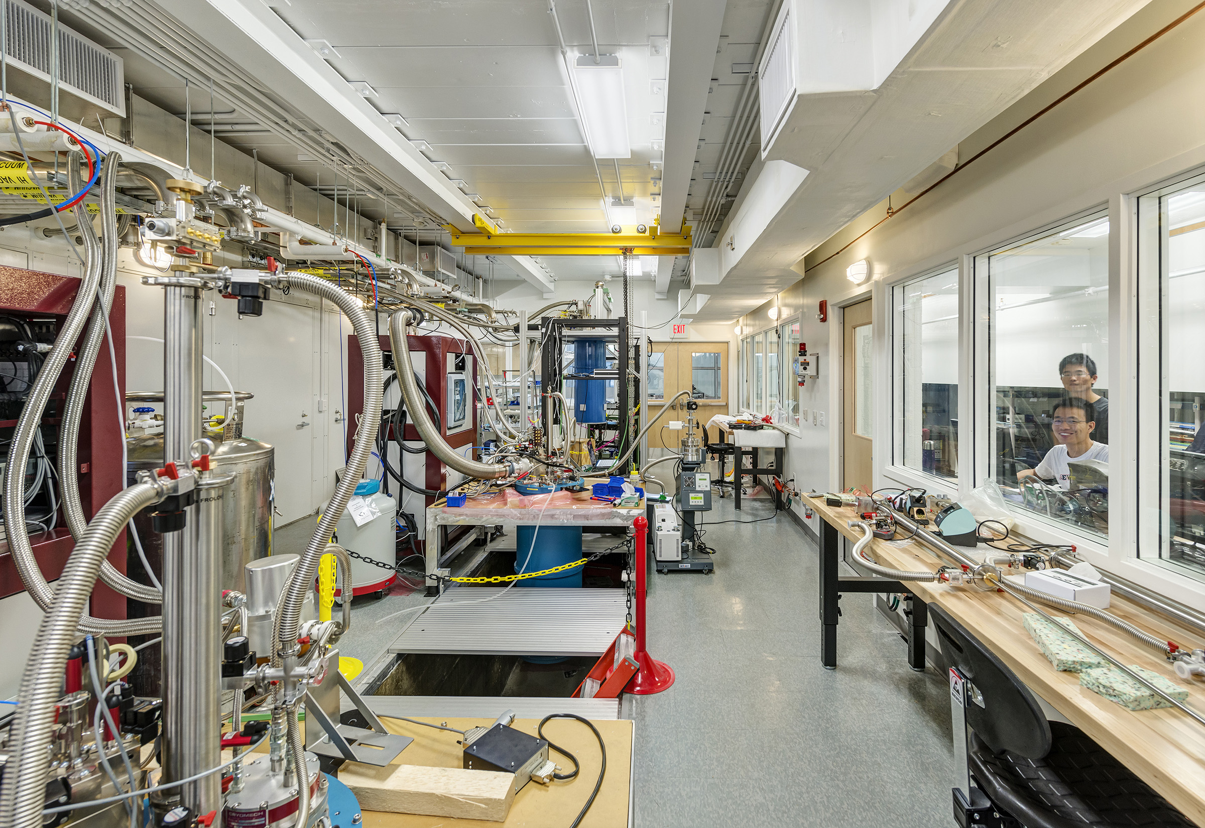
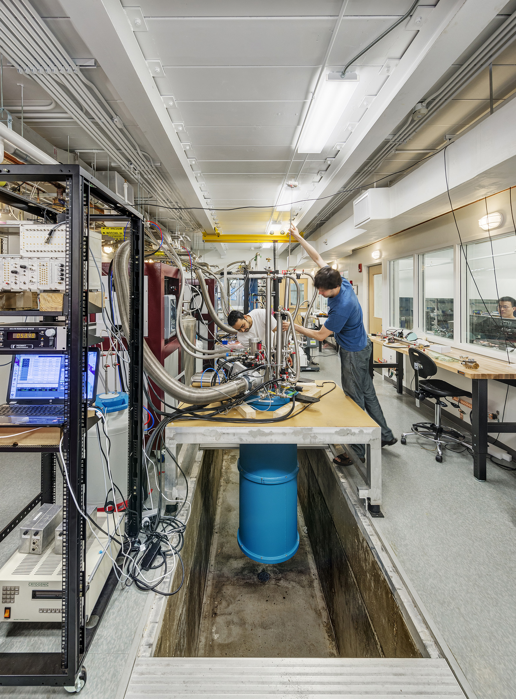
© Wilson Architects Inc., Anton Grassl / Esto
One problem with buying two identical fridges is how do you tell them apart. Well, one simple way, a long tradition in cryogenic labs, is to name your cryostats, you know, like ships. This process is not going too well so far in our group, and I take full responsibility.
Well, it did not help that fridges came from Leiden Cryogenics with creative names like Frolov1 and Frolov2. It is of course not an unreasonable idea to name fridges after famous physicists, for example Sheldon and Leonard, but who is going to want to work in a theorist-fridge? (Keep in mind the terrible Pauli effect)
Neither did it help that the fridge labeled “2” arrived first. That created a lot of confusion as in -Which fridge are we talking about? The first one, you know – that arrived the second… For a while they were called Left and Right, but of course that depends on the point of view… They were also called ‘Vector’ and ‘Solenoid’ after the kind of magnet that they had, until the magnets got swapped. And it became a nightmare. The second fridge, you know the vector, I mean solenoid, the one that used to be a vector and that arrived the first and so it is called the second.
To make things absolutely clear, people started saying ‘The fridge that is closer to the pink box’ as opposed to ‘the one in the center of the lab’. But the pink box has wheels, and this is not an elegant naming system at all. One of my students proposed ‘Ying’ and ‘Yang’ as in the opposites that somehow attract and coexist, but it gave me the wrong feeling to have metaphysical forces acting on delicate scientific equipment.
So. I have to make a decision. I will call one of them Narwhal, because of the top-loading probes that stick out like a tusk of a narwhal.
And the other one shall be called… Narwhal2? Oh boy, here we go again.
The way we do research is reminiscent of the timeless show “Fraggle Rock”. In the world of fraggles, there are fraggles, which mostly go about their silly business. And there are also doozers. Those are creatures that are focused, motivated and constantly building beautiful scaffolding of some transparent substance. They fill space with this scaffolding in no time. The twist is, that this scaffolding is very tasty, and fraggles love it – so they just grab it and eat it. In one episode fraggles start feeling bad about destroying the magnificent scaffolding castles built by doozers, so they stop doing it. This makes doozers very upset, because as it turns out, they enjoy making fraggles happy, and want their structures to be eaten.

In our research we work and fully depend on material scientists who grow magnificent structures, such as semiconductor nanowires. Growing nanowires is science with a twist of magic, because a lot of it is about methodical yet creative tuning of growth parameters that produces qualitatively new classes of materials. In a recent example, I was fortunate to collaborate with material scientists from Eindhoven on the characterization of a new type of nanostructure they produced – a semiconductor nanocross.

These crystals come about when two nanowires grow into each other. The Eindhoven group have achieved a high degree of control and reproducibility in producing these nanocrosses out of InSb. Our experimental team in Delft then contacted all four legs of a cross with metals and superconductors and found them to be of high electronic mobility and in the quasi-ballistic transport regime. Nanocrosses can find applications in research on Majorana fermions and topological quantum computing. Qubits based on Majorana fermions consist of several Majoranas, and to change the qubit state one has to switch Majorana positions. A recent theory found that this cannot be done in a single nanowire, and at least a nanowire T-junction, or a cross, is required.
Inspired by a recent conference on quantum computation
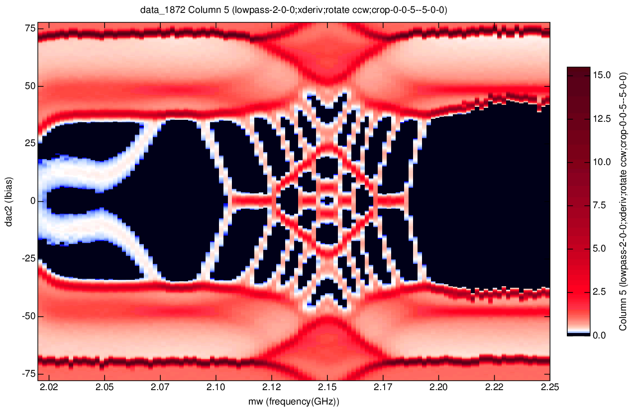
Can you guess what is being measured? (Hint: not Majorana, though these days any funny-looking graph is presented as such)
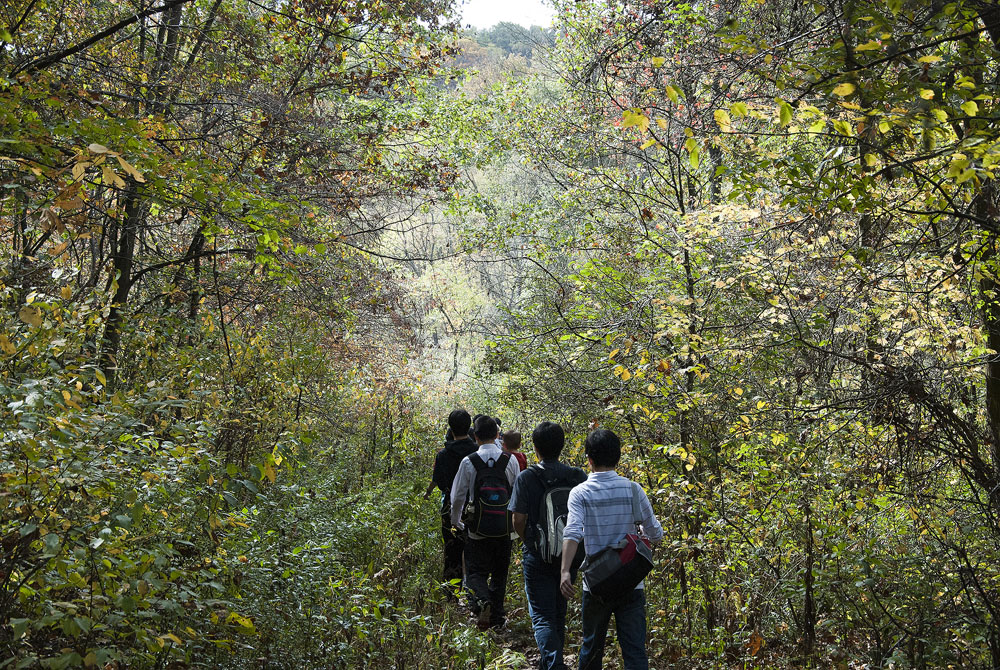
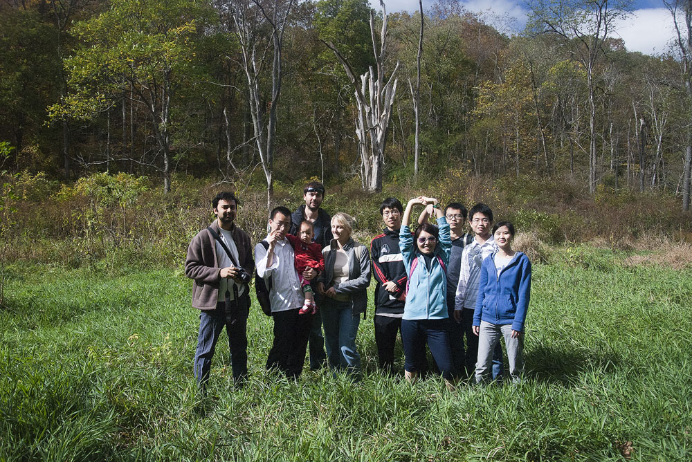
A couple of weeks ago we took advantage of Indian summer to walk around in a nearby Raccoon Creek park. Most of my group and friends/families joined.
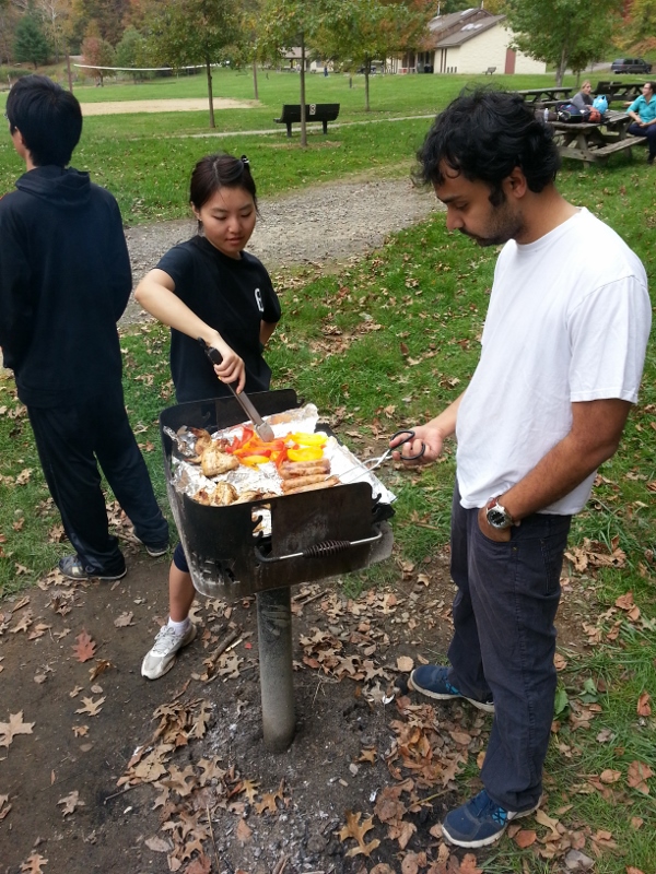
And barbeque after the hike was timely, though there was way too much food:

Pennsylvania is very picturesque in the Fall!
This graph shows the flow of electrical current without developing a voltage (supercurrent) through a semiconductor coupled to two superconductors. The size of the maximum supercurrent (called critical current) can be controlled by a voltage on a nearby electrode (gate).
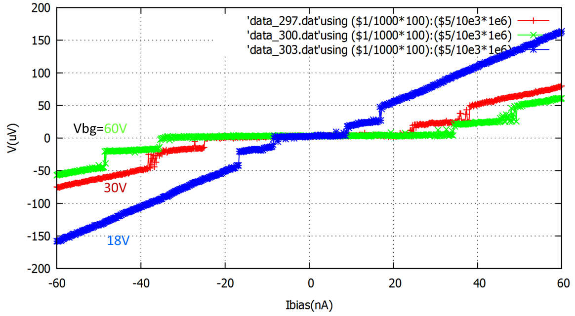
Seeing this effect is important for building up to Majorana fermion experiments. It has been reported first in this paper from 2005. So we are steadily catching up with state-of-the-art (Coulomb blockade from a couple of posts ago was first demonstrated in the 1980-ies).
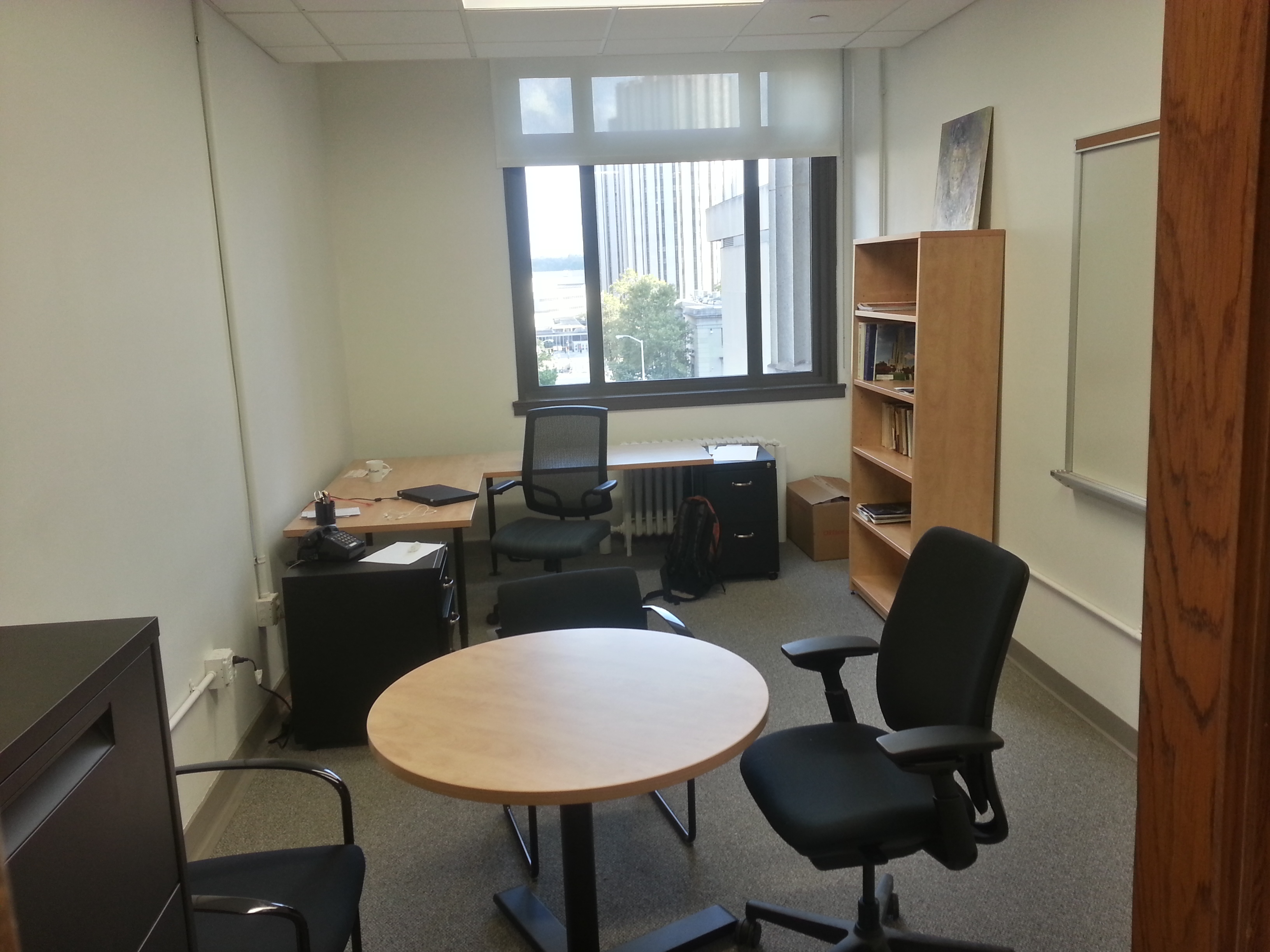
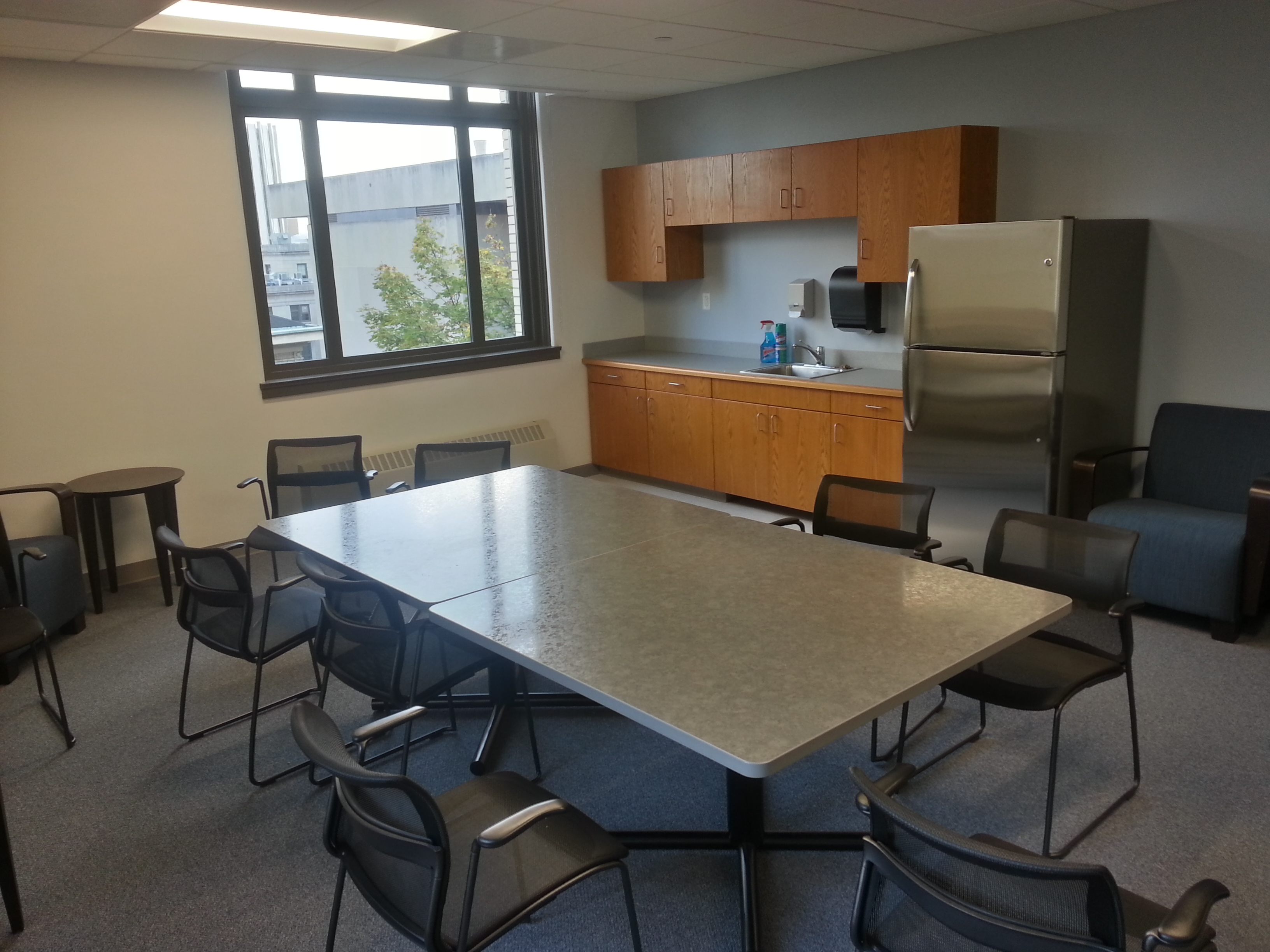
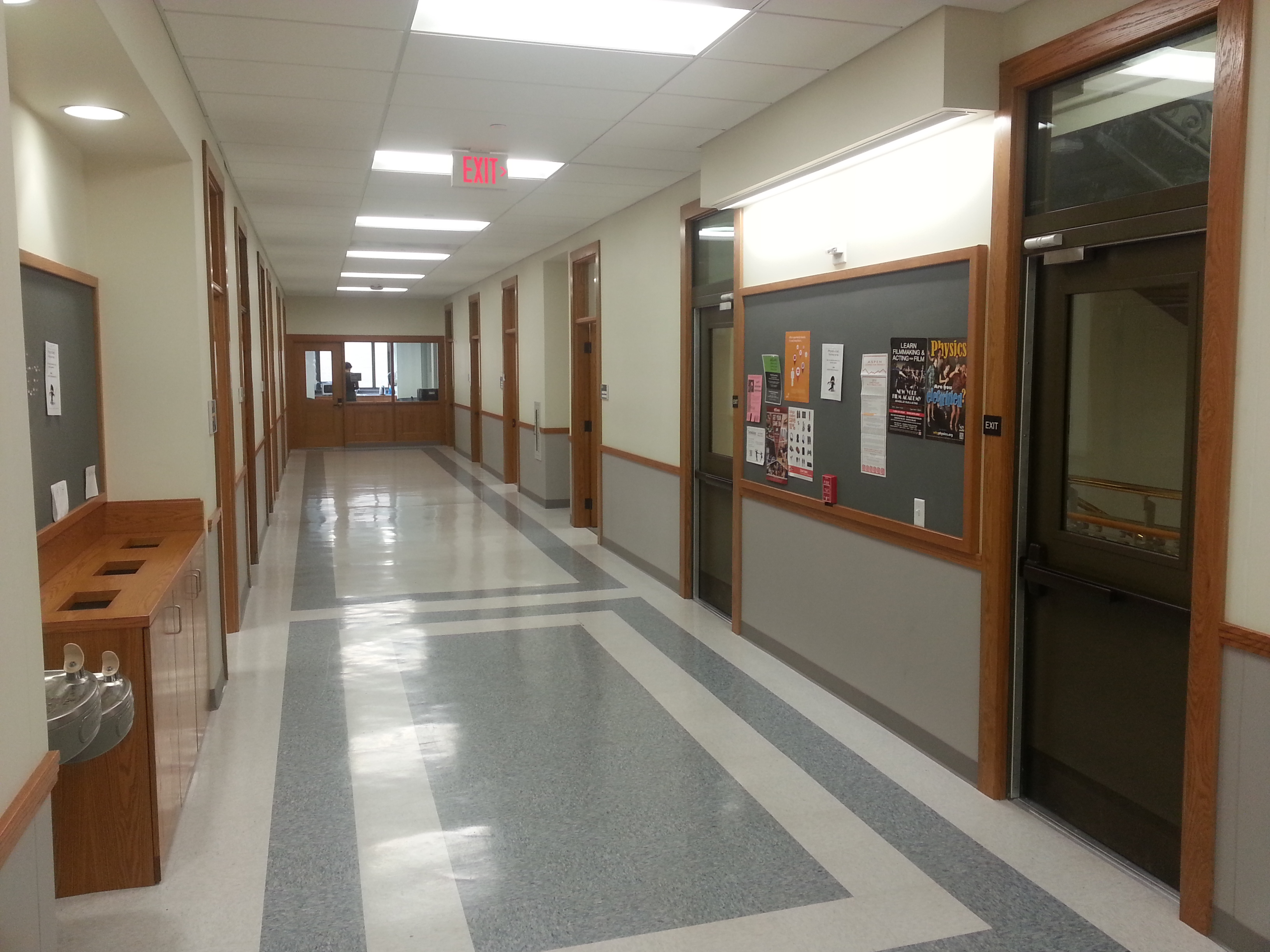
Here are a few snapshots from the Condensed Matter floor of Allen Hall, freshly renovated home of the Physics Department at Pitt.
My office:
Condensed Matter Lounge Center. The kitchen counter is where our espresso machine is going as soon as we get 220 V power for it:
Hallway, graduate student hall is at the far end.

You must be logged in to post a comment.